
IC Design
Digital system design and system-on-chip integration and verification is one of the core competencies of Integro Silicon. Design of special digital blocks with power, timing, or area constraints could be the target of any product specification. Our team is highly experienced in deployment of industry-standard tools including Synopsys and Cadence. We bring final working products in fast and reliable process with a small number of iterations.
- Turn-key Solution for IC/Module Design
- Design from Specifications to Chip Layout
- Chip-level Integration of a system including:
- Processors
- HW accelerators
- Signal processing engines
- Encryption engines
- Third-party IPs
Competitive Advantages
- Skillful and agile team
- Existing silicon-proven IP cores
- Ready-to-go setup and flow
- Lower risk of operation
- Lower OPEX
- Low engineering cost
- 15+ years of successful IC design in different process technologies
Assist you to specify the requirements for your systems targeting ASIC flow.
The simulations with specially developed EDA tools give precise predictions about the function and efficiency of final ASICs.
Integro Silicon specialized in IC design brings your idea from concept down to GDS. We can offer the following design services at very low cost:
1- Complete RTL-GDS flow including but not limited to:
a. HDL design and verification
b. Frontend synthesis
c. Backend flow (Layout generation, extraction, timing analysis, power estimation,…, final integration)
d. Formal verification
2. Collaboration with analog/RF team on mixed design
3. Embedded software development (Bare-metal/Linux)
4. Hands-on ARM architecture (Processor, AXI/AMBA, slave design, verification)
5. Skillful on FPGA (Zynq, Kintex, Ultrascale)
6. Hardware accelerator
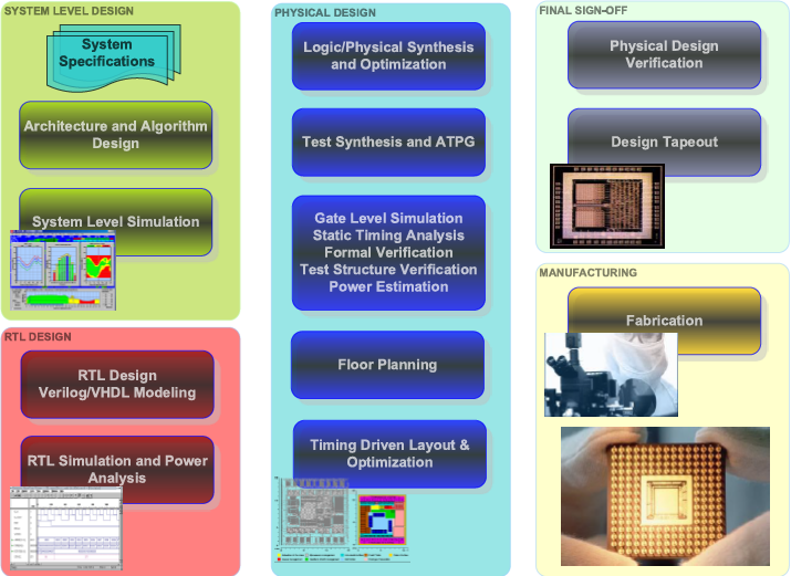
Design Flow
Our design flow comprises all detail and fine-grained processes from concept to RTL and then to GDSII that is delivered to fabrication houses for manufacturing. Hands on industry leader tools from Cadence, Synopsys and Mentor gain a higher level of reliability and helps realization of first-time working silicon for almost all of our products.
Verification is one of the key elements in our flow including exact timing and power analysis as well as handling signal integrity issues that have become serious problems in DSM era. Also, for board-level verifications and prototyping we employ Xilinx FPGAs.
- Feasibility study
- High-level Block diagram
- Cycle-accurate modelling (Matlab flow)
- HDL coding
- Functional simulation
- System integration
- FPGA synthesis/P&R/Emulation mainly for digital part
- Logic verification using UVM
- Extensive testbenches for System-level verification
- Constraint Development
- ASIC synthesis.
- DFT Insertion & ATPG
- Static Timing Analysis & Closure
- Place and Route
- Logic Equivalency Checking
- Analog/RF integration
- Design rule check
- Total LVS (Digital+Analog/RF)
- Final GDS & Sign-off
Post-fab activity
- Package selection
- Test board PCB design
- PCB assembly (chip + peripherals)
- Load testbenches
- Physical/Environment test (power, speed, temperature,…)
Chip Fabrication Model
For manufacturing of the ASIC chips, Integro uses a fabless model which gives access to a different range of chip fabrication technologies. Digital and mixed-signal technologies are used to fabricate the chip products. The chips are manufactured using advanced technology services of reputable foundries.