Projects
Integro design focuses in the following area
Application Processors
Network processors
Development Platforms
IP cores
Digital-signature SOC
IoT
Internet Broadband Gateway
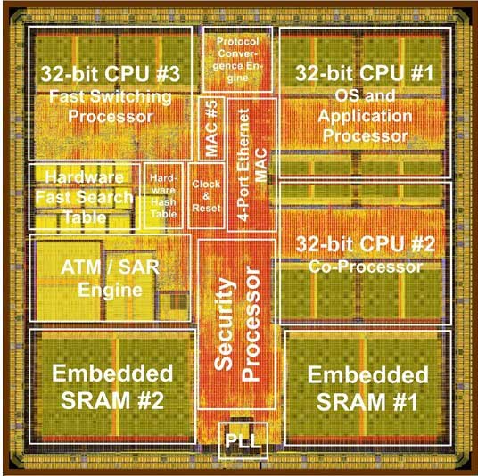
IBG is a two-chip integrated ARM system with accompanying dedicated hardware that includes a combination of various peripheral and network interfaces. It has been designed to operate as a gateway in many applications. The IBG CPUs are two 32-bit ARM946 processors which are connected to the rest of the system via ARM interconnect matrix (multi-layer AHB). All busses in the system are AHB (Advanced High-performance Bus), except two APB (Advanced Peripheral Bus) busses, which prepare the connectivity among some lower-speed peripherals and the system. IBG utilizes two ARM Dual Master DMA controllers to transfer data among various parts in the system. An off-chip Digital Signal Processor (DSP) can be added to the system through an external DSP interface, and it can bring many voice features into the system. IBG includes a dedicated piece of high-performance hardware that has been tailored to program DMAs of the system as well as providing basic layer-2 switching control functions of the switching fabric. IBG enjoys a parallel, distributed and run-time reconfigurable interconnecting architecture that allows system builders to explore numerous configurations for their under-development systems. While it supports fully connected interwoven blocks for resource sharing, and is possible to be governed by one single processor or bus master, on the run can be partitioned into totally separated and isolated building blocks and components. Eight parallel hardware threats are supported within the system. This will allow different OEMs provide consumer devices with an order of magnitude difference in performance and functionality based on the effort that they put on, or release during system development and code optimization. It supports many interfaces such as Fast Ethernet and ADSL UTOPIA as well as low bit-rate peripherals.
Major blocks of the chip are listed below
- Four Fast Ethernet links for local area
- L2/3 managed switching
- Embedded hardware accelerated security mechanisms
- ADSL and Fast Ethernet as broadband network interfaces
- Interfaces include USB, E1, PCMCIA, UART, HPI/SPI for DSP connection, Smart Card connector
- DDR SDRAM as packet, code and data memory
- Custom high-speed communication processor
- Optimized embedded operating system (Linux)
- Web-based management
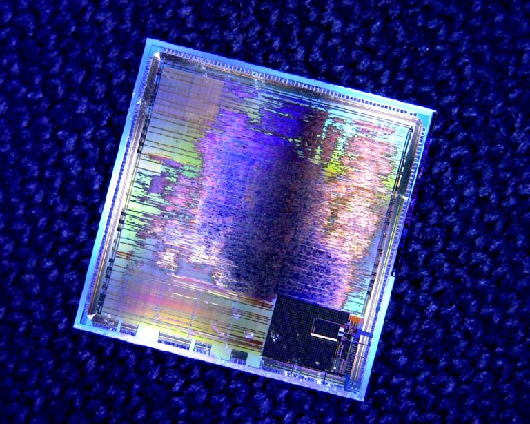
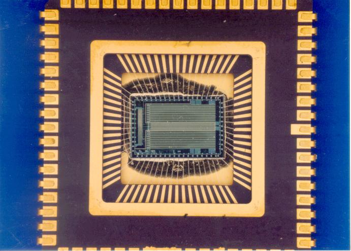
Digital Signature Chip
DSC is a 32-bit secure microcontroller equipped with RSA-2048 accelerator suitable for PC or cellular phone connectivity through USB port. It features a 128KB high-speed internal Flash and a 16KB ITCM, 16KB DTCM, and a rich set of peripherals.
It comprises a complete hardware system for security functions such as asymmetric cryptography engine RSA 512/1024/2048 bit, symmetric AES 256 bit, and various hash functions such as HMAC, SHA1/2, and MD5. RSA security accelerator performs the entire job without lengthy software interactions, resulting in a fast and low-overhead RSA operation. This also prevents the valuable flash memory area to be occupied by software codes developed for security functions.
Applicaton
- USB secure token
- Digital signature
- One-time password
- Smart cards
- Security accelerator
- POS Terminals
- Internet of Things (IoT)
- General purpose processing
Features
• ARM9 Processor
- 5-stage pipeline architecture
- Instruction/Data Tightly Coupled Memory (TCM)
- High speed 32b adder/multiplier
- 16x32b register set
- 16KB low latency instruction memory (ITCM)
- 16KB low latency data memory (DTCM)
- 8KB security RAM
• 128KB embedded high-speed flash
- CPU clock pause policy during flash access
- 8/16/32b access
- Instruction fetch capability
- Programmable timing adjustment on different clock speed
- Greater than 10 years data retention
- Sector endurance: 100,000 Cycles
• Internal Regulator
- Input voltage: 3.3v
- Output voltage: 1.25v,1.8v, 3v
- Power on Reset generation
• Brown-out detection
- Useful in battery operated devices
- Robust operation in sensitive applications
• Internal PLL
- Lock time: 1.5us
- Input range: 1-14MHz
- Multiplication: x6,x7,x8
- Output range: 6-112MHz
- Bypass mode
• True Random Number Generator (TRNG)
- Configurable sampling clock and number of rings
• Power Management
- Independent clock management under software control
- Clock dividers: x2-x8
- Clock gating unused devices
- Clock pausing for slow modules
• Interrupt Controller
- Individually maskable
- Priority based
- Vectored interrupt sources
- External interrupt source
• Timers
- 4xIndependent counter
- 2xup counter
- 2xdown counter
- Interrupt generation
• Watchdog
- 32-bit programmable counter
- Interrupt generation
- Internal hardware reset generation
• GPIO
- 16-bit general purpose input/output pins
- Boot mode selection over selected pins
- UART
• SPI
- Master mode Serial Peripheral Interface
- Programmable clock up to 50MHz
- Separate TX/RX FIFO
• USB
- USB Full Speed (12Mb) Device
- 2x Interrupt endpoint
- 2x Bulk endpoint
- 1x Control endpoint
- 240B FIFO
• RSA Crypto Engine
- 512-1024-2048 bit operation
- 10 sec average 2048b key generation time
- 2 sec average 2048b signature
- Integrated TRNG for secure key generation
• AES/DES/Hash Hardware accelerator
- 256 bit AES engine
- DES/3DES accelerator
- MD5/SHA1/2 message digest
- 16×32 bit input/output FIFO
Low-power IoT Chip
- Based on ARM Cortex M0
- Extremely low power operation
- Battery powered
- Multi-mode tracking system
- Mixed mode RF/Analog/Digital chipset
- 4Mbit internal SRAM, 2Mbit Internal ROM
- SPI, UART, Timers, Watchdog interfaces
- Fully digital baseband design
Application
Location-based services
Smartwatches
Healthcare and monitoring
Personal Navigation Devices
Asset Tracking
IP Portfolio